Laserlab started as a photoplotting shop in 1988 with a single Optrotech Laser Photoplotter.
In the more than twenty years since then we have shipped hundreds of thousands of photoplots
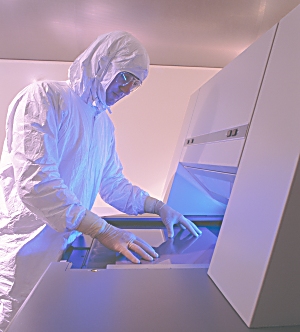
to thousands of customers. We currently have three laser photo plotters located in our class
1000 clean room facility in San Diego, California.
We are located right across the street from a Fedex hub. This allows us to ship your job as
late as 5:30PM Pacific time (8:30PM Eastern) for arrival at your facility the next morning.
Make sure to provide adequate ventilation when using this product.
Sprayway SW206 is flammable, so keep away from ignition sources.
Store films in LDPE bags (one is provided with each photoplot).
Store in a cool, clean place between 30% and 60% humidity.
Sizes
Smallest standard sheet size is 12x18" (maximum image 10x16")
Largest standard sheet size is 26x37" (maximum high-resolution image 24x35",
maximum very-high-resolution image 22x30")
Standard sheet sizes are 12x18", 16x20", 20x24", 24x28", and 26x37"
Image Resolutions
Two image resolutions are available, high and very high.
High resolution is 4000 DPI or 1/4 mil. (6.35um)
minimum line width is 0.0015" (1.5 mils) (38.1um) for orthogonal lines
minimum line width is 0.003" (3 mils) (75um) for diagonal lines
minimum aperture size is 0.001" (1 mil) (25.4um)
recommended for all applications other than those requiring the highest possible
resolution. Applications include PCBs, silkscreens, high-frequency PCBs, Hybrid circuits,
chemically etched components with fine lines. etc.
Very High resolution is 8000 DPI or 1/8 mil. (3.175um)
minimum line width is 0.0005" (0.5 mil) (12.7um) for orthogonal lines*
minimum line width is 0.001" (1 mil) (25um) for diagonal lines
minimum aperture size is 0.0005" (0.5 mil) (12.7um)
recommended for microwave PCBs, hybrid circuits, chemically milled components,
microfluidics, gratings, low-resolution semiconductor wafer masks, etc.
* Certain restrictions apply when making lines of minimum size. Orthogonal lines and spaces
are easier to make than diagonal ones. Lines running parallel to the fast scan axis of the
photoplotter are the best quality.
File Formats
Native file format is Extended Gerber RS-274X or Gerber RS-274D*.
Acceptable formats include AutoCAD .dwg and .dxf, Gerber, and HPGL.
Conversion from other CAD formats is available. Please call.
* Preferred format is Gerber RS-274X. There may be a surcharge for loading and verifying
Gerber RS-274D data.